


Analog Circuit Noise: Causes, Analysis, and Practical Design Solutions
Find the Problem and Designing It Out!
Noise is one of the most persistent problems in analog circuit design because it is present even when the circuit is working exactly as intended. A sensor may produce a small, meaningful signal, while every resistor, transistor, amplifier, power rail, cable, and circuit board trace contributes unwanted electrical variation around it. If the desired signal is large, that variation may be harmless. If the signal is small, the same noise can obscure measurements, trigger false decisions, reduce dynamic range, or make an otherwise correct design appear unreliable.
The good news is that noise is not usually a mysterious failure. It can be modeled, budgeted, measured, and reduced. The key is to treat noise as a design requirement from the beginning rather than as a problem to investigate after the prototype is complete.

What engineers mean by noise
In an analog circuit, noise is an unwanted, unpredictable fluctuation in voltage or current. It is different from a deterministic interference signal, such as a periodic clock harmonic or a switching-converter ripple frequency, although interference and noise can appear together in a measurement. Noise is usually described statistically because its instantaneous waveform cannot be predicted precisely.
A useful first distinction is between signal amplitude and signal quality. A circuit can have plenty of gain and still have poor performance if it amplifies the noise along with the signal. The important question is not simply, “How much output voltage do I have?” It is, “How large is the desired signal compared with the unwanted variation over the bandwidth that matters?”
That relationship is commonly expressed as signal-to-noise ratio, or SNR:
SNR = desired signal power / noise power
A higher SNR means the circuit can distinguish the signal more reliably. In measurement systems, the required SNR may be set by accuracy, resolution, detection probability, or a downstream analog-to-digital converter. In control and automotive electronics, the limit may be set by the smallest change that must be detected without creating false events.

The major sources of analog noise
Several physical mechanisms contribute to analog noise. Understanding their behavior makes it easier to decide which design changes are likely to help.
Resistor thermal noise
Any resistor above absolute zero generates thermal noise because charge carriers move randomly. The voltage noise density of an ideal resistor is approximately:
en = sqrt(4 k T R) volts per root hertz
where k is Boltzmann’s constant, T is absolute temperature, and R is resistance. The total noise over a bandwidth B is approximately:
vnoise = sqrt(4 k T R B)
This equation reveals two important design facts. First, larger resistance produces more voltage noise. Second, wider bandwidth allows more noise power into the measurement. A resistor may be perfectly within its tolerance and still be a significant noise source.
Resistor noise also appears differently depending on the circuit topology. In an op-amp amplifier, the feedback and gain-setting resistors contribute noise at the output through the circuit’s noise gain. Very high resistor values may reduce loading, but they can increase thermal noise and make the circuit more sensitive to input current noise and board leakage.
Op-amp voltage and current noise
Operational amplifiers have internal noise sources that are usually specified in data sheets as input voltage-noise density and input current-noise density. Voltage noise is often written as en, with units of volts per root hertz. Current noise is often written as in, with units of amps per root hertz.
Input voltage noise behaves like a small noise-voltage source in series with the input. It is multiplied by the amplifier’s noise gain. Input current noise flows through the source impedance and creates an additional voltage noise. That means the best op amp depends on the impedance connected to its input. A device with excellent voltage noise may not be the best choice when the source impedance is high, because current noise can dominate.
The interaction between the op amp and the source impedance is one of the most common reasons that a noise calculation based only on the headline data-sheet voltage-noise number produces an incorrect result.
Flicker noise and low-frequency drift
At lower frequencies, many semiconductor devices exhibit flicker noise, commonly called 1/f noise. Its density increases as frequency decreases. This can be important in sensor interfaces, precision amplifiers, instrumentation, and systems that measure slowly changing signals.
A circuit that looks quiet at 10 kilohertz may perform poorly near 1 hertz or below. If the application measures temperature, pressure, position, or another slowly varying quantity, the designer must examine the low-frequency noise curve rather than relying on a single wideband noise specification.
Power-supply and environmental noise
Not all unwanted variation originates inside the signal path. Power supplies, digital clocks, switching regulators, motors, relays, radio transmitters, and neighboring circuits can couple energy into an analog design. Coupling may occur through conducted paths, common impedance, electric fields, magnetic fields, or radiated electromagnetic energy.
Supply-rejection specifications describe how much of a supply disturbance appears at the output, but they do not eliminate the need for good power distribution. A supply bypass capacitor placed far away may be much less effective than a properly selected capacitor placed directly at the device pins. Similarly, a shield or ground plane can help in one layout while creating an unintended return-current path in another.
Why bandwidth matters so much
Bandwidth is one of the most powerful noise controls available to the designer. Random noise power accumulates across frequency. If a circuit accepts twice as much bandwidth, it generally accepts more total noise, even if the noise density stays constant.
This is why “more bandwidth just in case” is often a poor design habit. If the signal of interest occupies 5 kilohertz, a 500-kilohertz analog bandwidth may provide no useful information while admitting ten times more noise bandwidth. The exact integrated-noise relationship depends on the filter shape, but the general principle is simple: do not amplify frequency content that the system does not need.
Bandwidth must be considered at several levels. The op amp’s closed-loop response, the sensor interface, any anti-alias filter, the analog-to-digital converter, and the digital processing chain all affect the total noise. A later digital filter cannot recover dynamic range that was already lost when excessive analog noise entered the converter.
Noise gain is not always signal gain
A particularly important op-amp concept is noise gain. Signal gain describes how the desired differential input signal is amplified. Noise gain describes how an input-referred voltage noise source is amplified by the feedback network. In a non-inverting amplifier, the two gains are often the same. In an inverting amplifier, they are not.
For an inverting amplifier with input resistor Rin and feedback resistor Rf, the signal gain magnitude is Rf/Rin, while the noise gain is:
noise gain = 1 + Rf/Rin
For example, an inverting amplifier with a signal gain of minus 10 has a noise gain of 11. The op amp’s input voltage noise, input bias-current noise converted through impedance, and several resistor-noise contributions are amplified according to that noise gain. Ignoring this distinction can lead to an optimistic noise estimate.
Noise gain also affects stability and bandwidth. Compensation components, input capacitance, and feedback-network parasitics can create peaks that increase noise in particular frequency ranges. A circuit can therefore have a respectable low-frequency noise calculation but still show excess integrated noise because of a high-frequency gain peak.
Build a noise budget before choosing parts
A noise budget is a structured estimate of how much each source contributes to the total. The objective is not to predict every electron. It is to identify the dominant terms and verify that the total stays below the system requirement.
A practical first pass should include:
Sensor or source noise
Op-amp input voltage noise
Op-amp input current noise multiplied by source impedance
Thermal noise fromresistors
Reference and bias-source noise
Power-supply noise and converter ripple
Expected bandwidth and filter shape
Layout-related coupling and interference
Temperature range and worst-case operating conditions
Independent random noise sources are usually combined by root-sum-square rather than by direct addition. If three uncorrelated sources contribute n1, n2, and n3, the total is approximately:
ntotal = sqrt(n1^2 + n2^2 + n3^2)
This has a useful design implication: reducing a small contributor does very little if one source dominates. If the largest source is ten times greater than the next largest, redesigning the smaller source may have almost no visible effect. Find the dominant term first.

Practical ways to reduce noise
Select the op amp for the actual source impedance
Choose an op amp using the complete application context, not a single marketing number. Compare voltage noise, current noise, 1/f noise, input bias current, input capacitance, input common-mode range, gain bandwidth, and supply-current behavior.
For low-impedance sources, voltage noise may dominate. For high-impedance sources, current noise and resistor noise may be more important. A precision low-noise amplifier is not automatically the best choice if its input current noise interacts badly with the source network.
Use sensible resistor values
Reducing unnecessarily high resistor values can lower thermal noise and the voltage generated by input current noise. However, very low values increase loading and power consumption. The right choice is a system tradeoff involving noise, loading, bias current, power, gain, and bandwidth.
Keep high-impedance nodes short and clean. They are more vulnerable to leakage, capacitive coupling, contamination, and electric-field pickup.
Limit bandwidth intentionally
Use an analog low-pass filter when the signal does not require the full amplifier bandwidth. Place filtering where it protects the next stage and prevents unwanted noise from entering an ADC. Consider the filter’s noise gain and op-amp stability, not just its nominal cutoff frequency.
A filter should be selected from the real signal spectrum and sampling plan. If the signal contains important transients, an overly aggressive filter may distort the measurement. The design goal is controlled bandwidth, not minimum bandwidth at any cost.
Improve supply bypassing and return paths
Place local bypass capacitors close to the op-amp supply pins. Provide a low-impedance return path appropriate for the frequency range of interest. Separate noisy switching-current loops from sensitive analog inputs, and avoid forcing high-current digital returns through the reference path of a low-level analog circuit.
Grounding is not simply a matter of connecting every ground point to the nearest copper. Current follows impedance, which varies with frequency. At higher frequencies, a short, wide return path may be more important than a long “direct” trace. At lower frequencies, shared resistance and connector drops may dominate.
Protect the layout from coupling
Keep sensitive input traces away from clocks, fast digital edges, switching nodes, inductors, motors, and high-current paths. Use differential routing when it improves rejection of common-mode interference. Guard high-impedance nodes where leakage is a concern. Avoid large loops that can receive magnetic interference.
Good layout cannot compensate for a fundamentally excessive noise budget, but poor layout can easily overwhelm a well-designed schematic.
Measure noise the right way
Noise measurement is easy to get wrong. An oscilloscope probe can add capacitance, pick up interference, or create a ground loop. A long ground lead can turn a quiet circuit into an antenna. The measurement instrument itself has a noise floor, and its bandwidth setting changes the observed result.
Start by defining what you are measuring: noise density, peak-to-peak noise over a stated bandwidth, RMS noise, or SNR. These values are not interchangeable. Always report the measurement bandwidth, input termination, gain setting, averaging method, and filtering.
Short the input or connect a known quiet source to separate circuit noise from source noise. Compare the measured noise with the instrument’s own noise floor. Use controlled grounding and shielding, and check whether the noise changes when nearby digital or switching circuits are enabled.
A frequency-domain measurement can be particularly revealing. A flat broadband floor suggests a different problem than a strong clock harmonic, a switching-regulator spur, or a rising 1/f region. The shape of the spectrum often points directly to the next design experiment.
Conclusion
Analog noise is unavoidable, but uncontrolled noise is usually a design choice. The most effective approach is to define the required signal quality, create a noise budget, identify the dominant sources, and then control them with appropriate component choices, gain structure, bandwidth, filtering, power distribution, and layout.
Good analog design does not attempt to make the circuit perfectly silent. It makes the noise predictable, measurable, and small enough that the system can perform its intended job. When the design is reviewed from the beginning with a noise budget in hand, the “mysterious noise problem” becomes a series of manageable engineering decisions—and the noise reaper loses another opportunity to surprise the team.
References
Texas Instruments, Noise Analysis in Operational Amplifier Circuits. Covers resistor thermal noise, op-amp voltage and current noise, noise gain, bandwidth, and total output-noise calculations.
Analog Devices, MT-047 Tutorial: Op Amp Noise. Explains op-amp noise models, Johnson noise, source-impedance tradeoffs, noise-source combination, and 1/f noise.
Keysight Technologies, Spectrum and Signal Analyzer Measurements and Noise. Provides background on noise measurements, bandwidth, averaging, instrument noise floors, and measurement limitations.
Horowitz, Paul, and Winfield Hill, The Art of Electronics, 3rd ed., Cambridge University Press, 2015. A broad reference for practical analog circuit design, feedback, amplifiers, filtering, and noise considerations.
Motchenbacher, C. D., and F. C. Fitchen, Low-Noise Electronic Design, Wiley, 1973. A deeper reference on physical noise mechanisms, low-noise component selection, and system-level noise design.
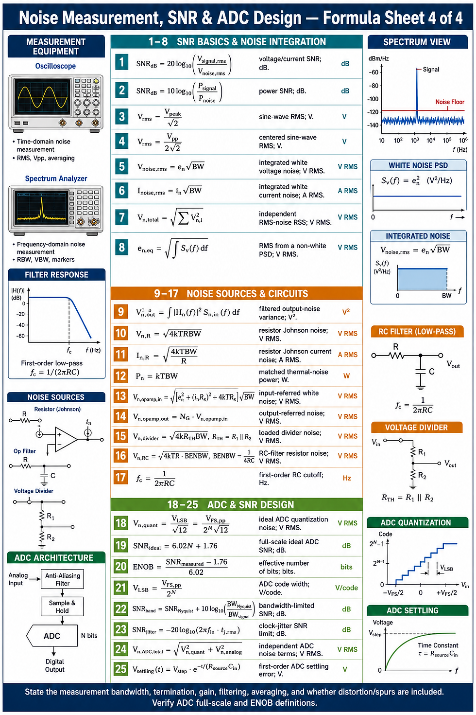
Noise Formula Sheets


Keywords
Primary keyword: analog circuit noise
Secondary keywords:
analog circuit design noise
op-amp noise
operational amplifier noise
noise gain
resistor thermal noise
Johnson noise
input voltage noise
input current noise
1/f noise
flicker noise
analog noise reduction
low-noise amplifier design
analog circuit noise budget
noise in sensor circuits
op-amp noise analysis
bandwidth and noise
analog circuit filtering
PCB layout for low noise
power-supply noise
signal-to-noise ratio
measuring analog noise


Comments